Team:ETH Zurich/Process/Validation
From 2011.igem.org
(→References) |
(→References) |
||
| Line 63: | Line 63: | ||
<span id="Ref1">[1] [http://www.elveflow.com/microfluidic/16-start-with-microfluidic http://www.elveflow.com/microfluidic/16-start-with-microfluidic]</span> <br> | <span id="Ref1">[1] [http://www.elveflow.com/microfluidic/16-start-with-microfluidic http://www.elveflow.com/microfluidic/16-start-with-microfluidic]</span> <br> | ||
| - | <span id="Ref2">[2] [http://www.springerlink.com/content/q744ww56gvg05753/#section=91916&page=1 Microfluidic Techniques | + | <span id="Ref2">[2] [http://www.springerlink.com/content/q744ww56gvg05753/#section=91916&page=1 | Microfluidic Techniques |
Methods in Molecular Biology, 2006, Volume 321, I, 17-21, DOI: 10.1385/1-59259-997-4:17, Chapter 3: Fabrication of Polydimethylsiloxane Microfluidics Using SU-8 Molds, Rabih Zaouk, Benjamin Y. Park and Marc J. Madou]</span> | Methods in Molecular Biology, 2006, Volume 321, I, 17-21, DOI: 10.1385/1-59259-997-4:17, Chapter 3: Fabrication of Polydimethylsiloxane Microfluidics Using SU-8 Molds, Rabih Zaouk, Benjamin Y. Park and Marc J. Madou]</span> | ||
Revision as of 14:59, 27 October 2011
Final Setup and Validation
This page presents description of our final channel design as well as description of its construction, which we did by ourselves. Our final channel is build out of polydimethylsiloxane (PDMS) and constructed with a technique called photolithography. We are also presenting the experiments we did to validate our setup and to show that it can work in practice.
Final Channel Design
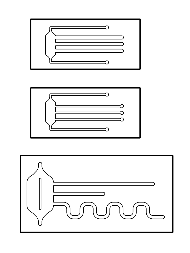
On the left is the design of our final microfluidic devices, which we made out of polydimethylsiloxane (PDMS). The three chips differ between themselves in their shape and dimensions. All of the channels on the chips have a reservoir attached to one end.
Dimensions of the chips:
- The size of the first two chips is 15 x 33 mm, the size of the last one is 23 x 46 mm.
- The width of the channels is either 0.5 or 1 mm
- Channel length:
- Large chip: (from top to bottom) 30 mm, 15 mm and ca. 60 mm
- Small chip: all 20mm
Final Channel Construction
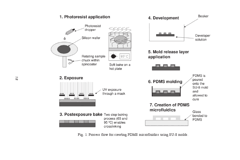
To construct the microfluidic channels, we used the technique photolithography. Photolithography is the photopatterning of channels from a mask (drawing of channels in 2D) and is based on the utilization of particular substances (photoresists) that become soluble to particular solvents after being exposed to UV light [1].
The technique is briefly like following: [2]
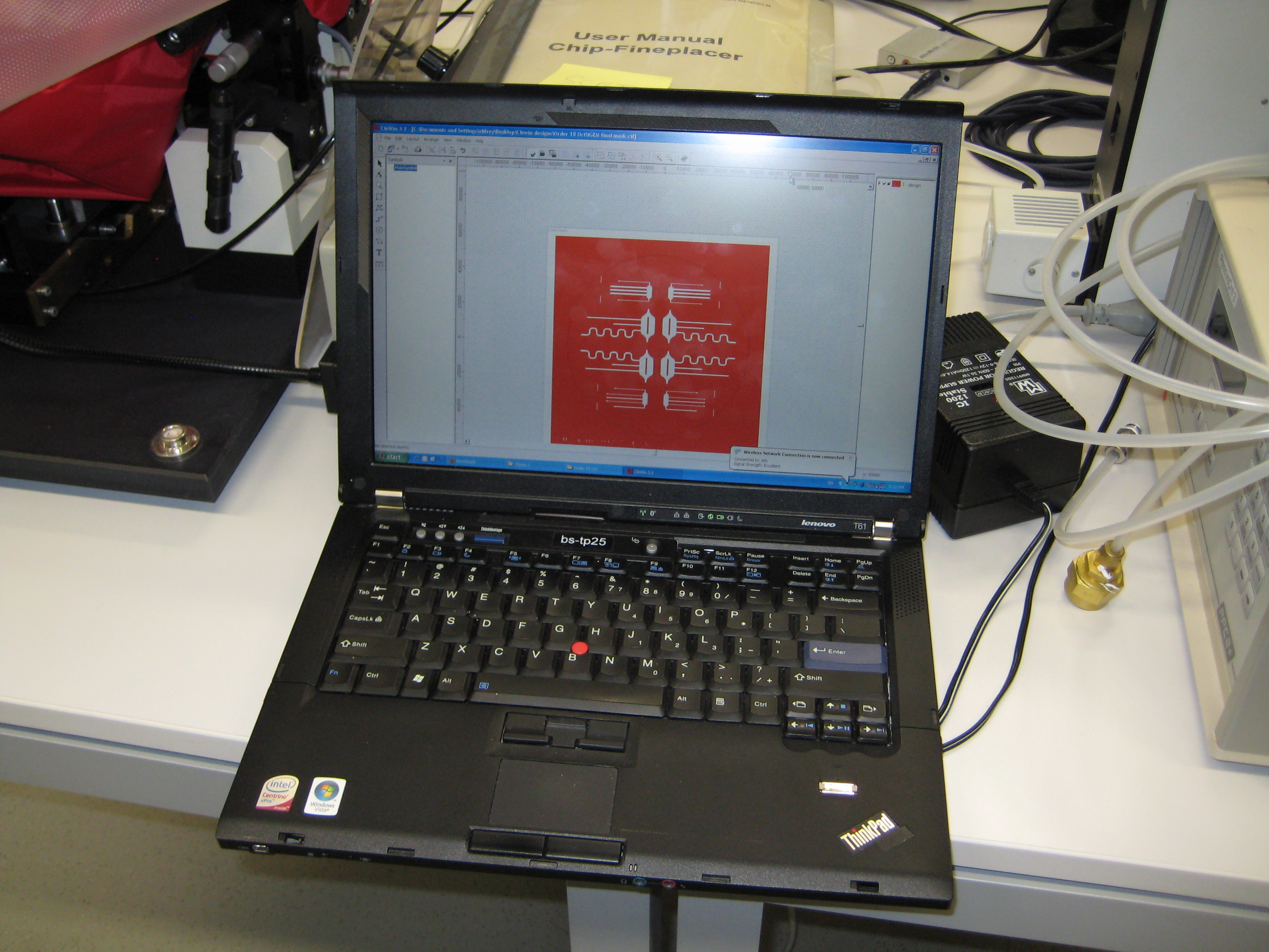
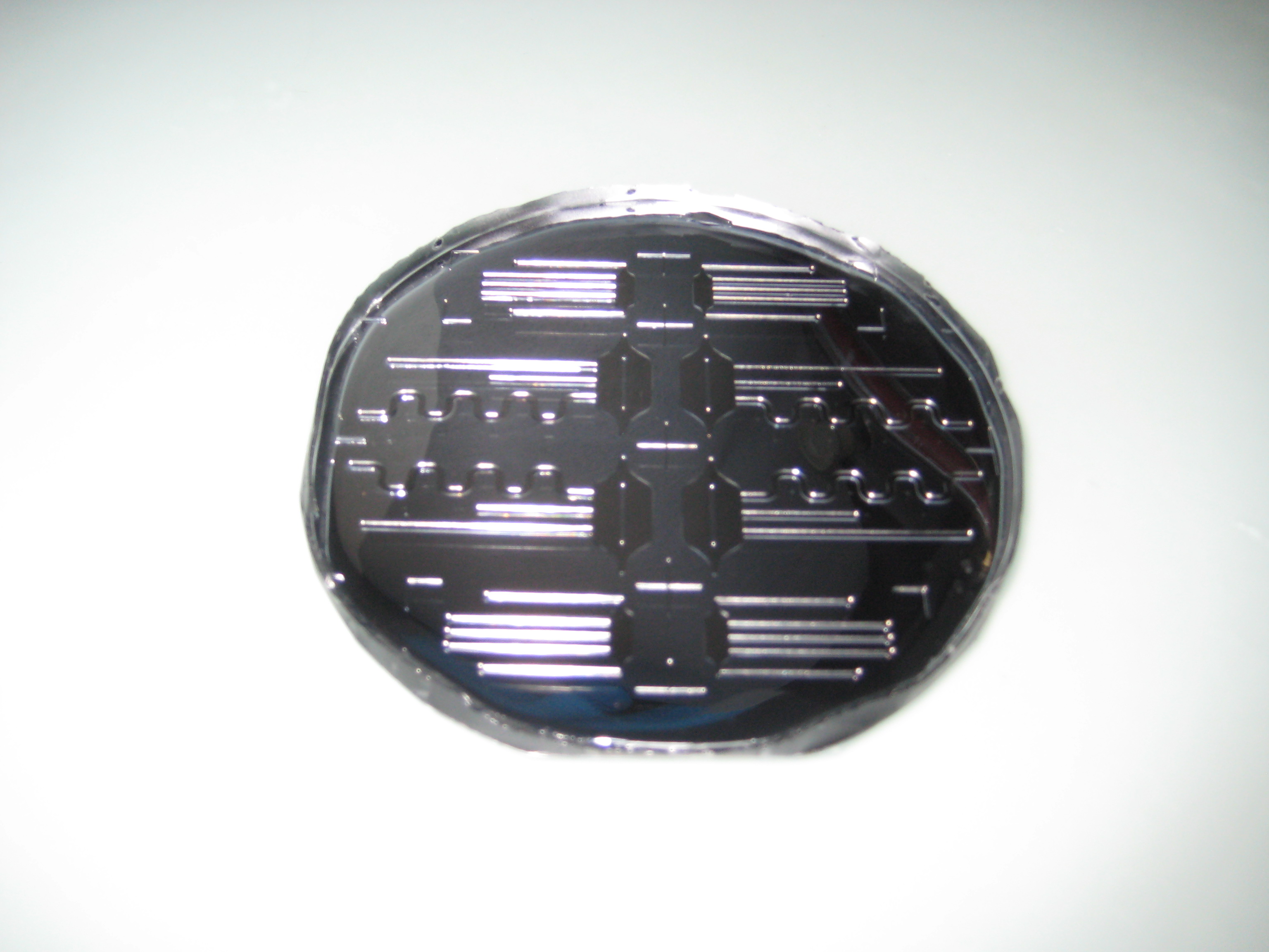
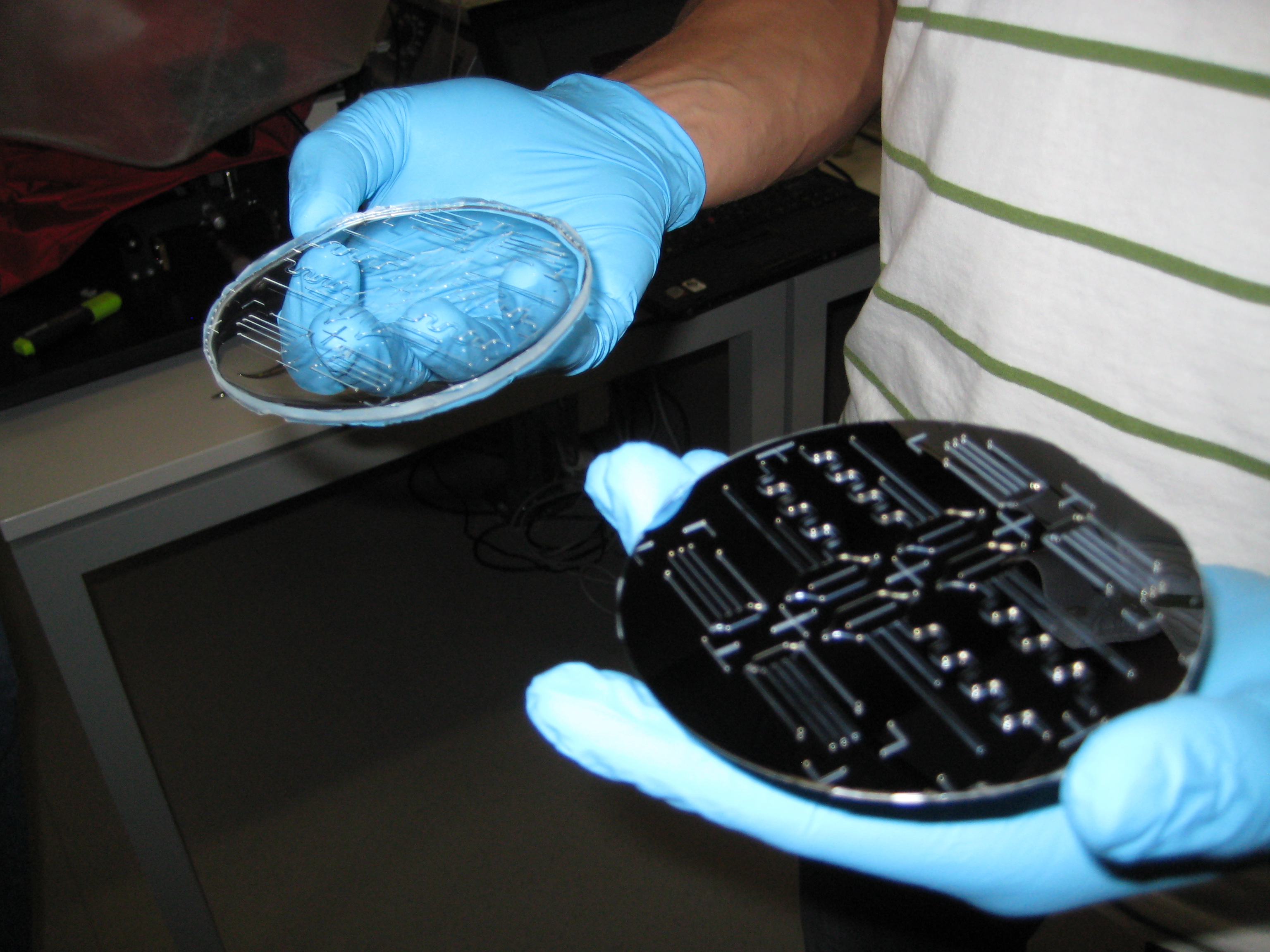
First, a mask for the microfluidic devises is made by printing the design on glass or quartz or simply on a regular transparency. Then, an SU-8 negative photoresist is spun onto a Si wafer until the final thickness of the photoresist is achieved. The transparency photomask is placed over the Si waver coated with photoresist and the photoresist is exposed under UV light, after which a postexposure bake is performed to crosslink selectively the exposed portions of the photoresist causing the solidification of the material. The sample is put in a beaker containing SU-8 developer to remove the unexposed SU-8. After the sample containing the xposed SU-8 only is is taken out of the baker and dried, PDMS is applied over the SU-8 mold and allowed to cure. SU-8 is removed and a glass is bounded to the PDMS. The channels are constructed. You can read more about the technique here.
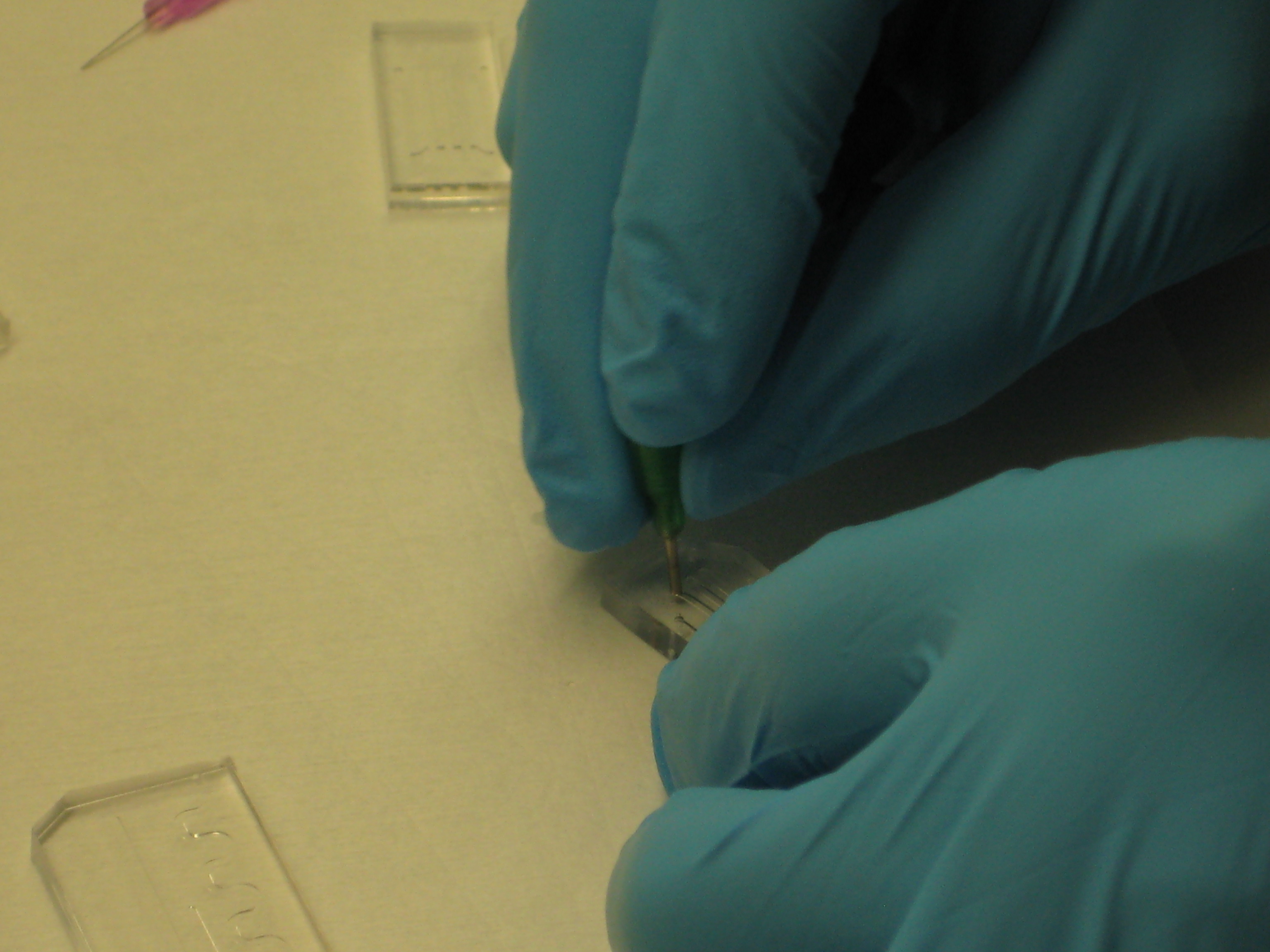
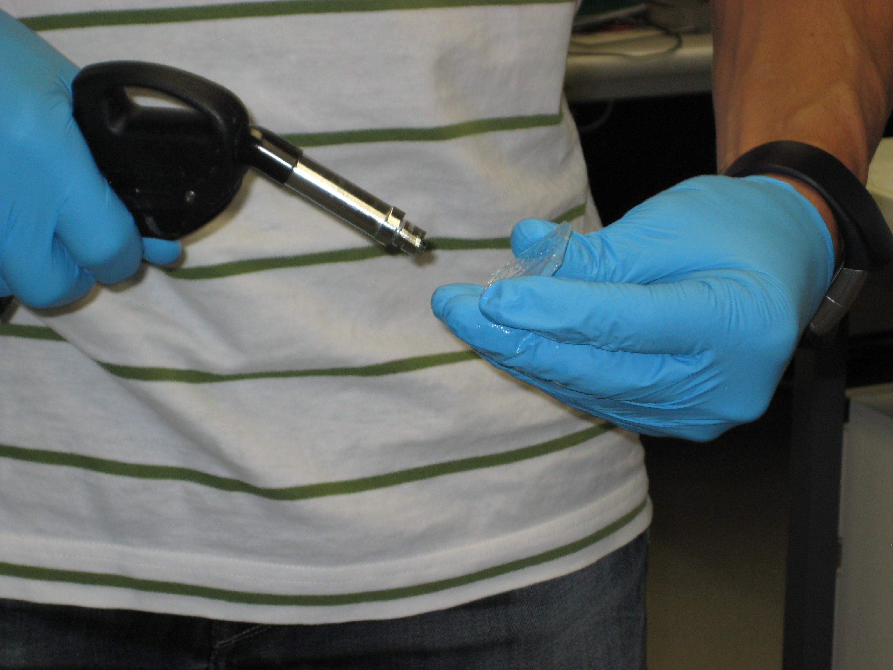
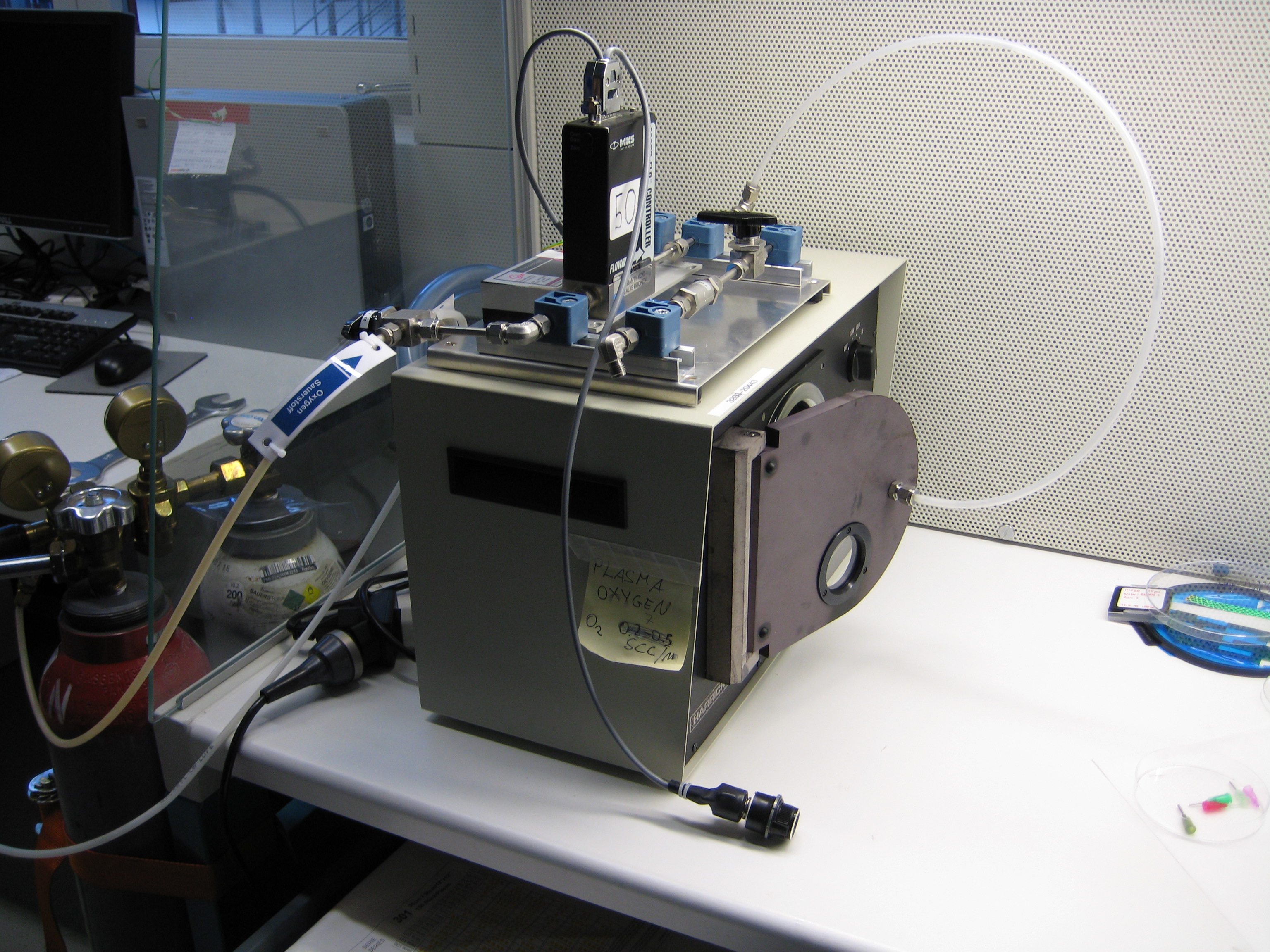
You can see below some photos of the channel building process:
Setup Validation
References
[1] [http://www.elveflow.com/microfluidic/16-start-with-microfluidic http://www.elveflow.com/microfluidic/16-start-with-microfluidic]
[2] [http://www.springerlink.com/content/q744ww56gvg05753/#section=91916&page=1 | Microfluidic Techniques Methods in Molecular Biology, 2006, Volume 321, I, 17-21, DOI: 10.1385/1-59259-997-4:17, Chapter 3: Fabrication of Polydimethylsiloxane Microfluidics Using SU-8 Molds, Rabih Zaouk, Benjamin Y. Park and Marc J. Madou]
 "
"


