Team:ETH Zurich/Process/Validation
From 2011.igem.org
(→Final Channel Construction) |
(→Final Channel Construction) |
||
| (46 intermediate revisions not shown) | |||
| Line 3: | Line 3: | ||
{{:Team:ETH Zurich/Templates/SectionStart}} | {{:Team:ETH Zurich/Templates/SectionStart}} | ||
= Final Setup and Validation = | = Final Setup and Validation = | ||
| - | '''This page presents description of our final channel design as well as description of its construction, which we did by ourselves. Our final channel is | + | '''This page presents description of our final channel design as well as description of its construction, which we did by ourselves. Our final channel is built out of polydimethylsiloxane (PDMS) and constructed with a technique called photolithography. Finally we performed some experiments in the channel in order to validate our design.''' |
{{:Team:ETH Zurich/Templates/SectionEnd}} | {{:Team:ETH Zurich/Templates/SectionEnd}} | ||
{{:Team:ETH Zurich/Templates/SectionStart}} | {{:Team:ETH Zurich/Templates/SectionStart}} | ||
| Line 11: | Line 11: | ||
| - | On the left is the design of our final microfluidic devices, which we made out of polydimethylsiloxane (PDMS). The three chips differ between themselves in their shape and dimensions. | + | On the left is the design of our final microfluidic devices, which we made out of polydimethylsiloxane (PDMS). The three chips differ between themselves in their shape and dimensions. On the left side of the chips, each design has a reservoir attached to one end of the channels. |
| Line 28: | Line 28: | ||
== Final Channel Construction== | == Final Channel Construction== | ||
| - | To construct the microfluidic channels, we used the technique photolithography. Photolithography is | + | To construct the microfluidic channels, we used the technique photolithography. Photolithography is done by photopatterning of structures by using a mask (drawing of channels in 2D) and is based on the utilization of particular substances (photoresists) that become soluble to particular solvents after being exposed to UV light [[#Ref1|[1]]].<br><br> |
| - | + | Hereafter a brief description of the photolithography technique: [[#Ref2|[2]]] | |
| - | + | ||
| - | + | First, a mask for the microfluidic devices is made by printing the design on glass or quartz or simply on a regular transparency. Then, an SU-8 negative photoresist is spun onto a Si wafer until the final thickness of the photoresist is achieved. The transparency photomask is placed over the Si waver coated with photoresist and the photoresist is exposed to UV light, after which a postexposure bake is performed to crosslink selectively the exposed portions of the photoresist causing the solidification of the material. The sample is put in a beaker containing SU-8 developer to remove the unexposed SU-8. After the sample containing the exposed SU-8 only is is taken out of the baker and dried, PDMS is applied over the SU-8 mold and allowed to cure. SU-8 is removed and a glass is bounded to the PDMS. The channels are constructed. [[#Ref2|You can read more about the technique here.]]<br><br> | |
| + | [[File:ETHZ_photolithography.png|800px|center|thumb|'''Figure 2:''' The process of designing the microfluidic devises. Graphic taken from [[#Ref2|[2]]] ]] | ||
| - | |||
| + | You can see below some photos of the channel building process: | ||
| + | <center> | ||
<gallery widths=240px heights=240px perrow=3 caption="Gallery: Producing the channel"> | <gallery widths=240px heights=240px perrow=3 caption="Gallery: Producing the channel"> | ||
File:ETH MasK mikro.png | File:ETH MasK mikro.png | ||
| Line 47: | Line 48: | ||
File:Plasmaofen.JPG | File:Plasmaofen.JPG | ||
</gallery> | </gallery> | ||
| - | + | </center> | |
| + | :::'''Figure 3: Fabrication of the PDMS channel''' | ||
{{:Team:ETH Zurich/Templates/SectionEnd}} | {{:Team:ETH Zurich/Templates/SectionEnd}} | ||
| Line 53: | Line 55: | ||
==Setup Validation== | ==Setup Validation== | ||
| + | [[File:ETH arabinose channel.jpg|900px|center|thumb|'''Figure 4: arabinose-induced GFP production in a 30 mm channel.''' The system was induced with a 1 %w/v arabinose solution in the reservoir on the left side of the channel. Pictures were taken 5 h after induction.]] | ||
| + | To test the different PDMS channels, we engineered an arabinose-dependent sfGFP reporter plasmid, with which ''e.coli'' BW27783 strain [[#Ref3|[3]]] was transformed. A liquid preculture was grown until an OD<sub>600</sub> of 1 was reached. Cells then were diluted by 1/5 in LB and 15 %w/v agar was added to the suspension. Then the suspension was poured into the channels and solidified afterwards. To induce GFP production, solutions with different concentrations of arabinose were added to the reservoir on one side of the chips. | ||
| + | |||
| + | Afterwards, the chips were incubated at 37 °C. Therefore, they were put into a petri dish filled with water. This should prevent evaporation and thus draining of the channels. We further sealed all the entrances to the channels for the same reason and also to avoid accidential dilution of arabinose in the reservoir. | ||
| + | Samples were taken after regular time periods. Pictures were taken by using a fluorescence microscope with an ecitation wavelength of 480 nm and an emission wavelength of 510 nm. As visible in figure 3 and 4, a gradient in GFP fluorescence could be observed as expected. | ||
| + | |||
| + | |||
| + | Thus we successfully designed a PDMS channel which is compatible with the SmoColi system, allowing us to do time course measurements with a fluorescence microscope over a longer span of time without risking to drain the channel. | ||
| + | |||
| + | |||
| + | [[File:ETHZ_arabinose_gradient.png|500px|center|thumb|'''Figure 5: Proof of principle''', arabinose-inducible GFP gradient created in the microfluidic PDMS device.]] | ||
| - | |||
{{:Team:ETH Zurich/Templates/SectionEnd}} | {{:Team:ETH Zurich/Templates/SectionEnd}} | ||
{{:Team:ETH Zurich/Templates/SectionStart}} | {{:Team:ETH Zurich/Templates/SectionStart}} | ||
| - | + | = References = | |
| + | |||
| + | <span id="Ref1">[1] [http://www.elveflow.com/microfluidic/16-start-with-microfluidic http://www.elveflow.com/microfluidic/16-start-with-microfluidic]</span> | ||
| - | <span id=" | + | <span id="Ref2">[2] [http://www.springerlink.com/content/q744ww56gvg05753/#section=91916&page=1 '''Microfluidic Techniques: Reviews and Protocols''', Shelley D. Minteer,<br> '''Chapter 3: Fabrication of Polydimethylsiloxane Microfluidics Using SU-8 Molds''', Rabih Zaouk, Benjamin Y. Park and Marc J. Madou]</span> |
| - | <span id=" | + | <span id="Ref3">[3] [http://mic.sgmjournals.org/content/147/12/3241/F4.expansion.html A. Khlebnikov, K. Datsenko, T. Skaug, B. Wanner and J. Keasling: Homogeneous expression of the PBAD promoter in Escherichia coli by constitutive expression of the low-affinity high-capacity AraE transporter, Microbiology, 2001, (147): 3241–3247]</span> |
{{:Team:ETH Zurich/Templates/SectionEnd}} | {{:Team:ETH Zurich/Templates/SectionEnd}} | ||
{{:Team:ETH Zurich/Templates/HeaderNewEnd}} | {{:Team:ETH Zurich/Templates/HeaderNewEnd}} | ||
Latest revision as of 01:56, 29 October 2011
Final Setup and Validation
This page presents description of our final channel design as well as description of its construction, which we did by ourselves. Our final channel is built out of polydimethylsiloxane (PDMS) and constructed with a technique called photolithography. Finally we performed some experiments in the channel in order to validate our design.
Final Channel Design
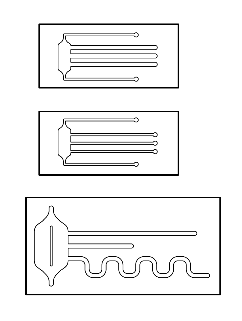
On the left is the design of our final microfluidic devices, which we made out of polydimethylsiloxane (PDMS). The three chips differ between themselves in their shape and dimensions. On the left side of the chips, each design has a reservoir attached to one end of the channels.
Dimensions of the chips:
- The size of the first two chips is 15 x 33 mm, the size of the last one is 23 x 46 mm.
- The width of the channels is either 0.5 or 1 mm
- Channel length:
- Large chip: (from top to bottom) 30 mm, 15 mm and ca. 60 mm
- Small chip: all 20mm
Final Channel Construction
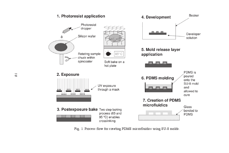
To construct the microfluidic channels, we used the technique photolithography. Photolithography is done by photopatterning of structures by using a mask (drawing of channels in 2D) and is based on the utilization of particular substances (photoresists) that become soluble to particular solvents after being exposed to UV light [1].
Hereafter a brief description of the photolithography technique: [2]
First, a mask for the microfluidic devices is made by printing the design on glass or quartz or simply on a regular transparency. Then, an SU-8 negative photoresist is spun onto a Si wafer until the final thickness of the photoresist is achieved. The transparency photomask is placed over the Si waver coated with photoresist and the photoresist is exposed to UV light, after which a postexposure bake is performed to crosslink selectively the exposed portions of the photoresist causing the solidification of the material. The sample is put in a beaker containing SU-8 developer to remove the unexposed SU-8. After the sample containing the exposed SU-8 only is is taken out of the baker and dried, PDMS is applied over the SU-8 mold and allowed to cure. SU-8 is removed and a glass is bounded to the PDMS. The channels are constructed. You can read more about the technique here.
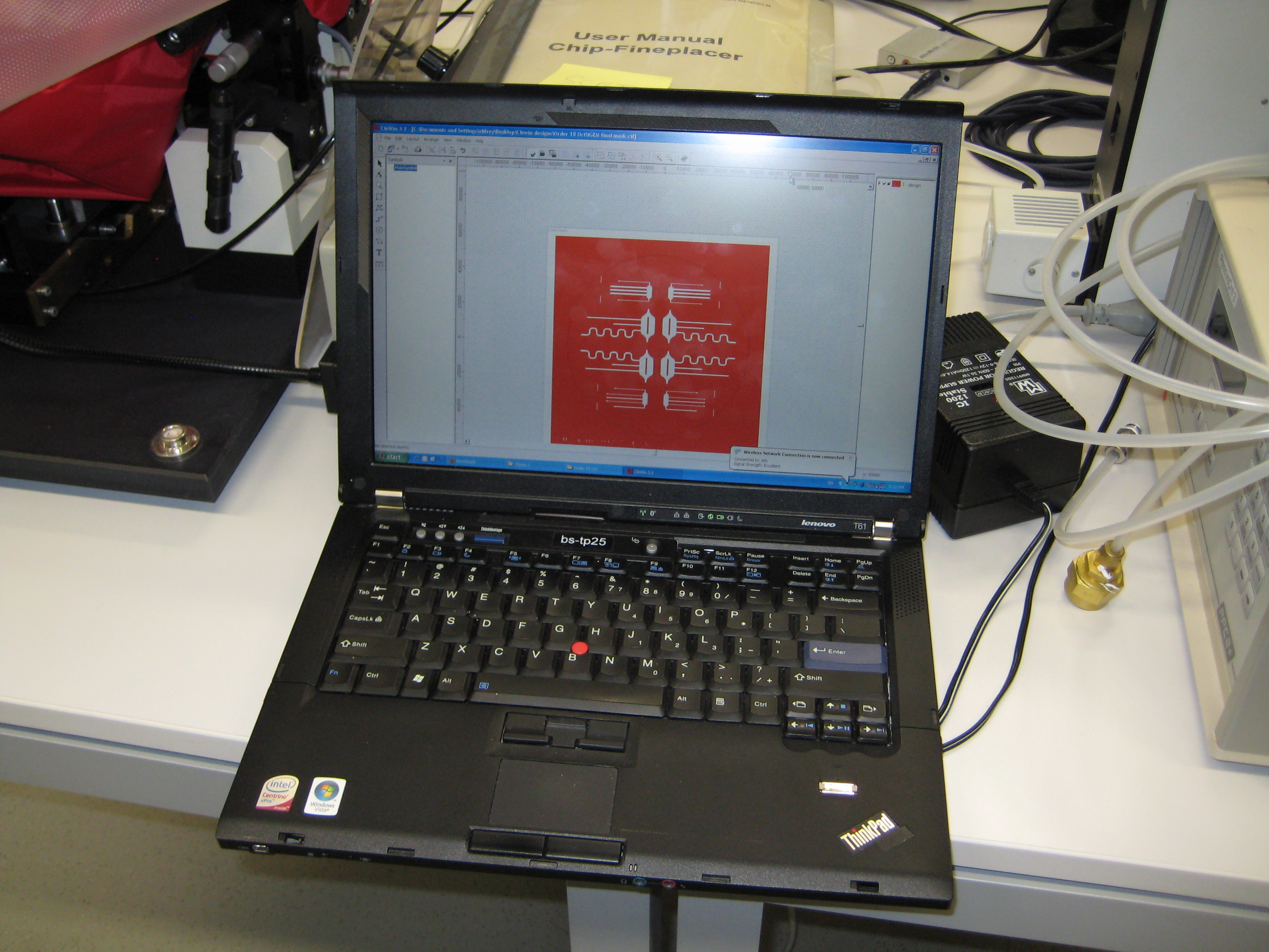
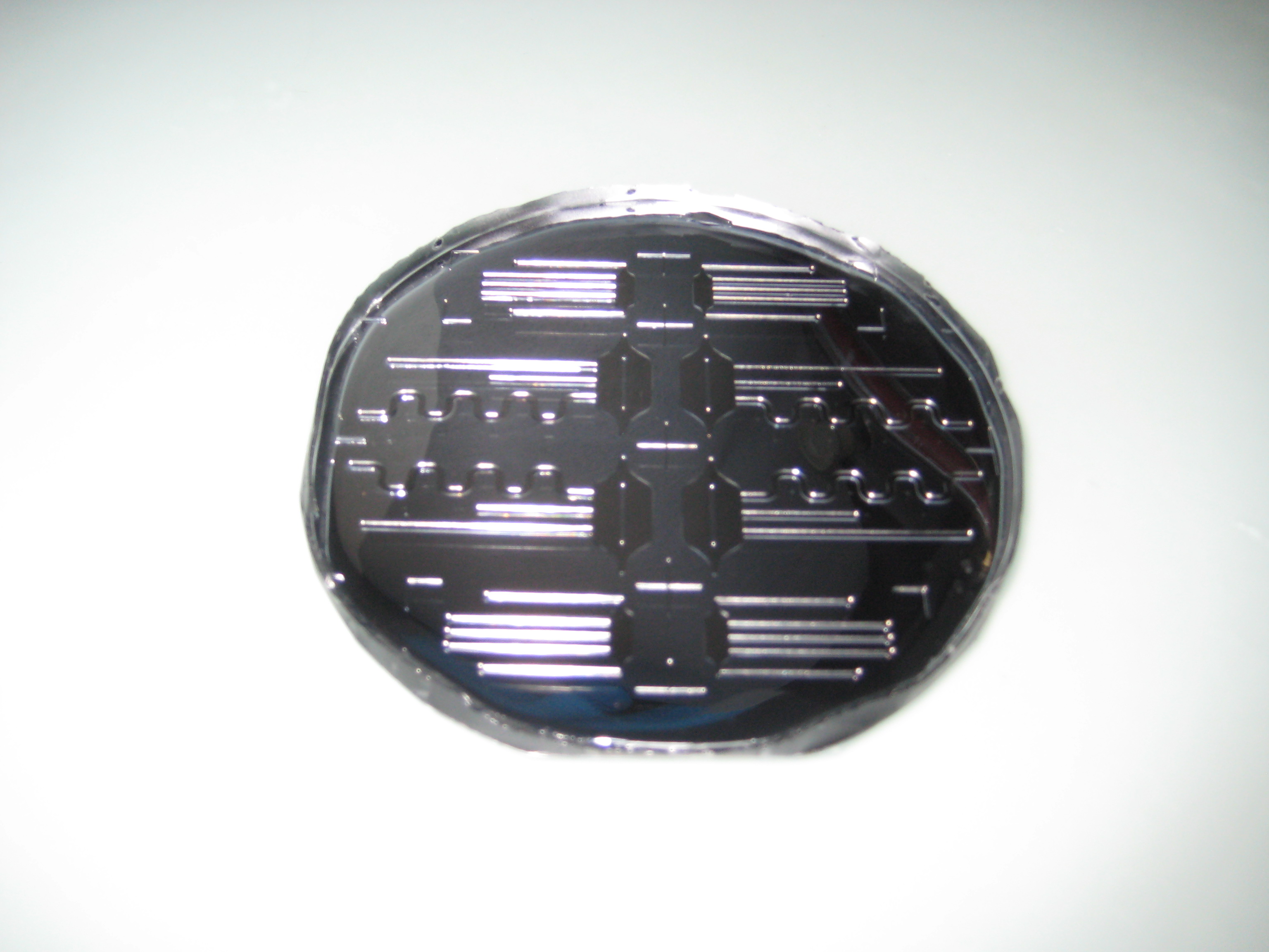
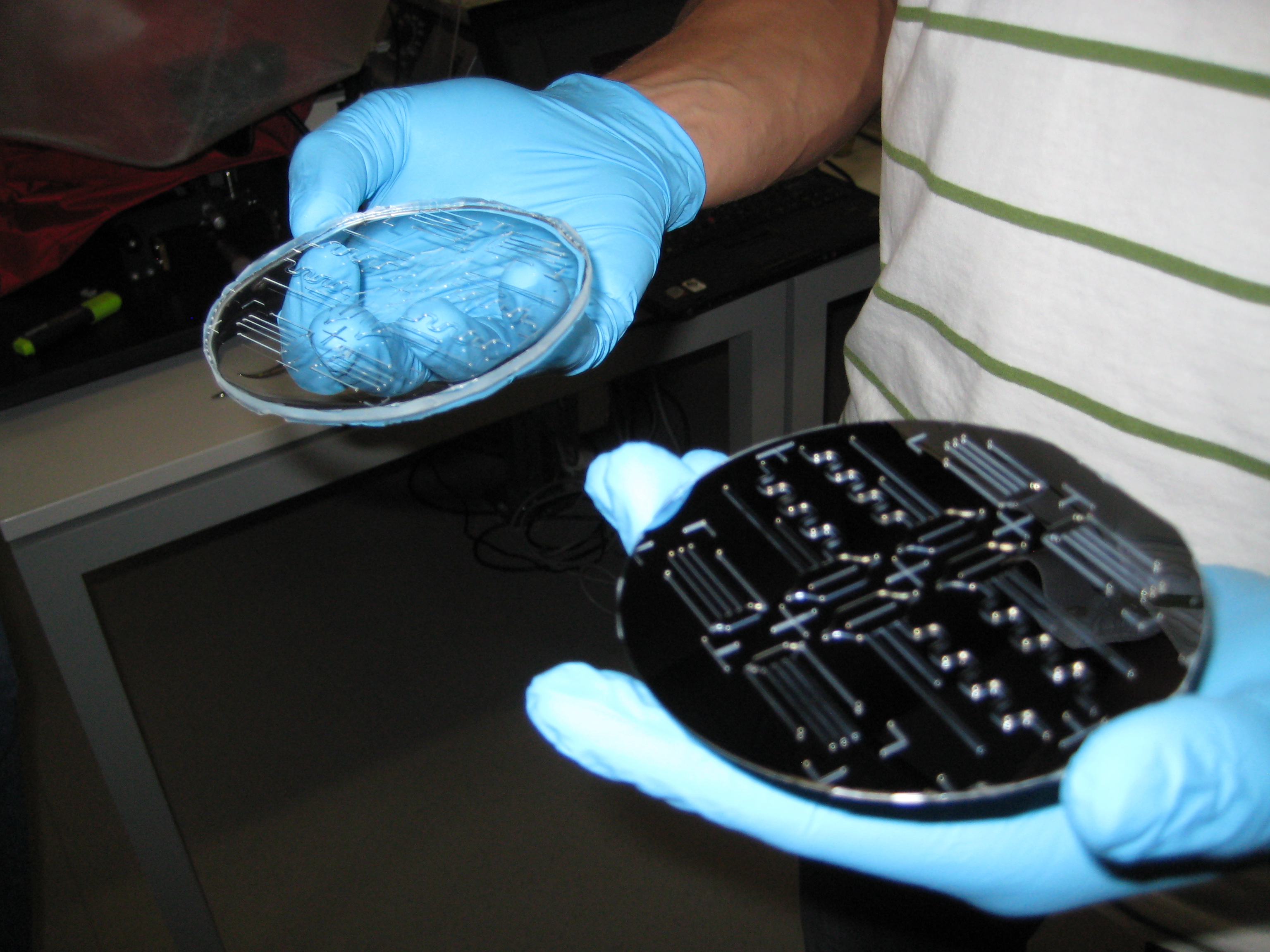
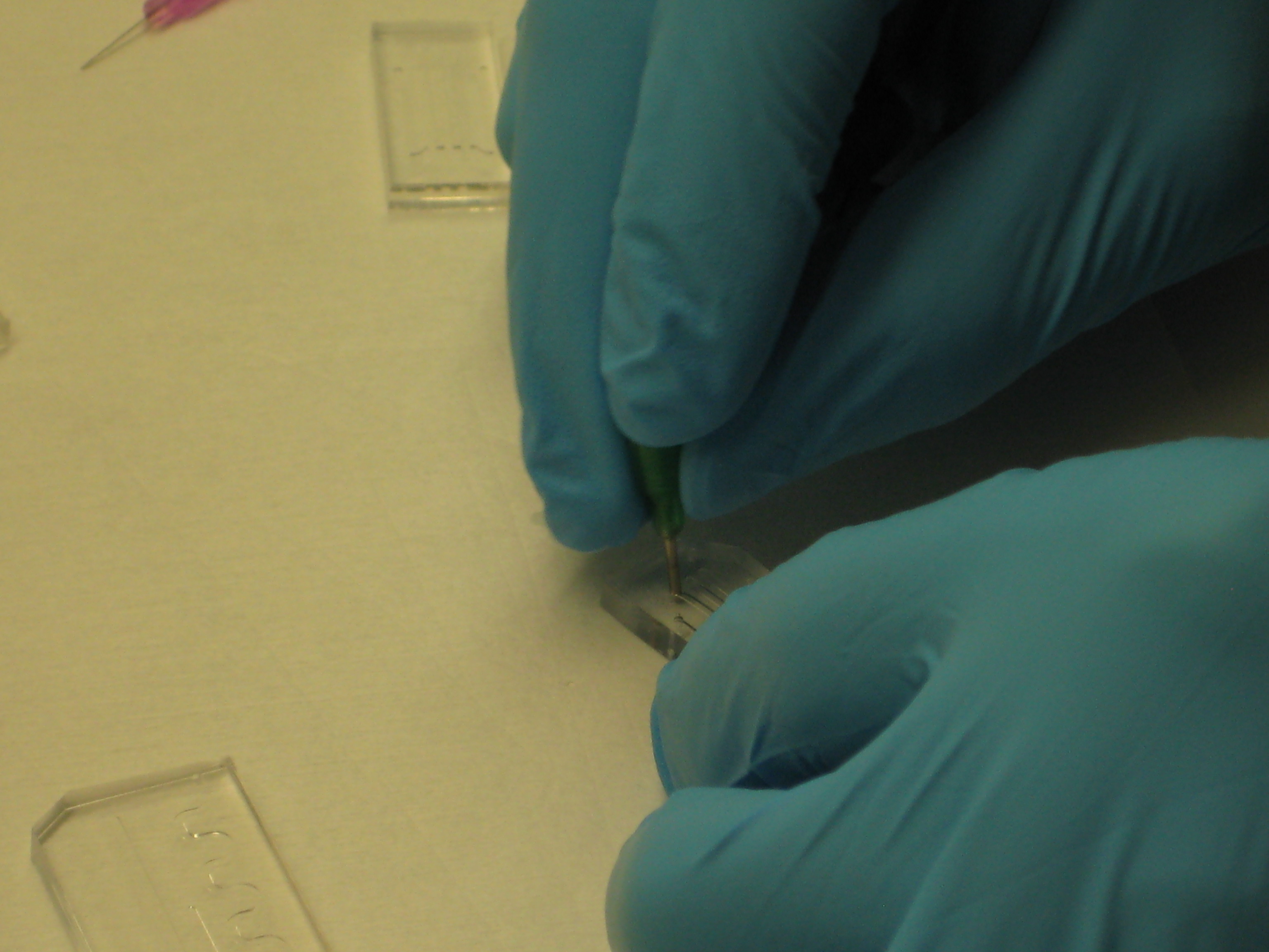
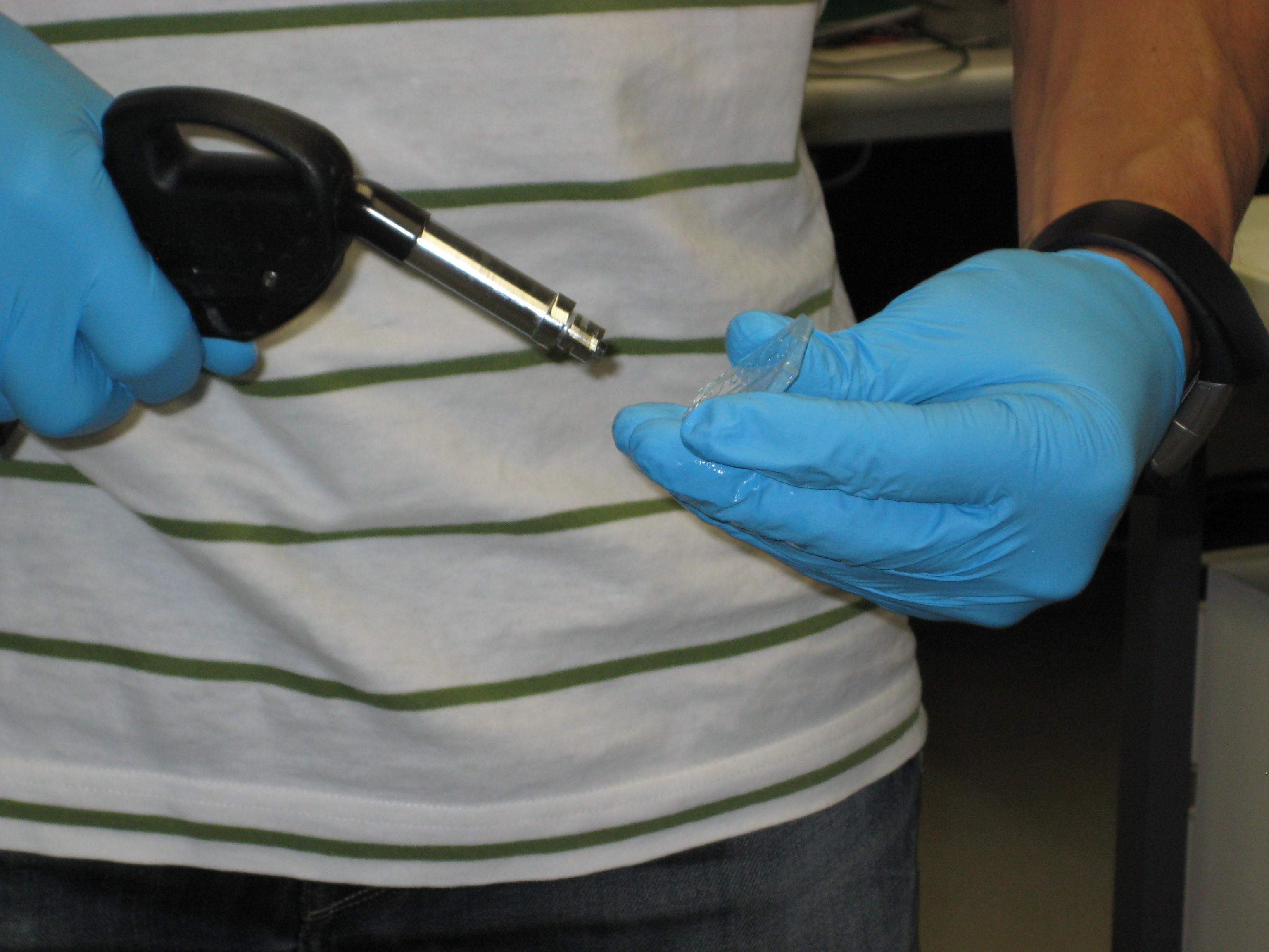
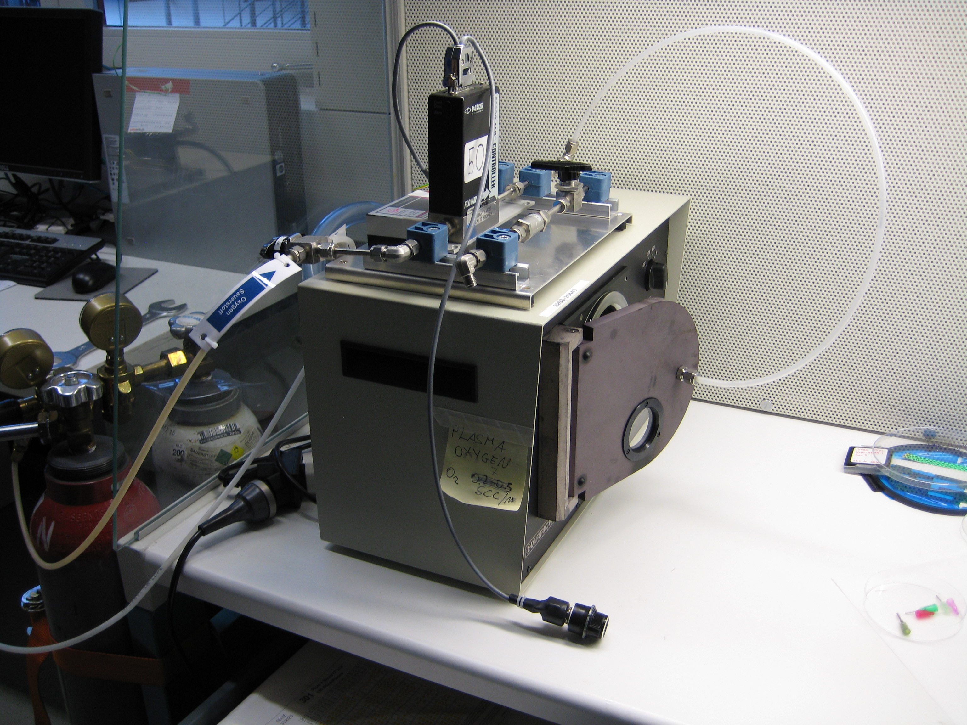
You can see below some photos of the channel building process:
- Figure 3: Fabrication of the PDMS channel
Setup Validation
To test the different PDMS channels, we engineered an arabinose-dependent sfGFP reporter plasmid, with which e.coli BW27783 strain [3] was transformed. A liquid preculture was grown until an OD600 of 1 was reached. Cells then were diluted by 1/5 in LB and 15 %w/v agar was added to the suspension. Then the suspension was poured into the channels and solidified afterwards. To induce GFP production, solutions with different concentrations of arabinose were added to the reservoir on one side of the chips.
Afterwards, the chips were incubated at 37 °C. Therefore, they were put into a petri dish filled with water. This should prevent evaporation and thus draining of the channels. We further sealed all the entrances to the channels for the same reason and also to avoid accidential dilution of arabinose in the reservoir. Samples were taken after regular time periods. Pictures were taken by using a fluorescence microscope with an ecitation wavelength of 480 nm and an emission wavelength of 510 nm. As visible in figure 3 and 4, a gradient in GFP fluorescence could be observed as expected.
Thus we successfully designed a PDMS channel which is compatible with the SmoColi system, allowing us to do time course measurements with a fluorescence microscope over a longer span of time without risking to drain the channel.
References
[1] [http://www.elveflow.com/microfluidic/16-start-with-microfluidic http://www.elveflow.com/microfluidic/16-start-with-microfluidic]
[2] [http://www.springerlink.com/content/q744ww56gvg05753/#section=91916&page=1 Microfluidic Techniques: Reviews and Protocols, Shelley D. Minteer,
Chapter 3: Fabrication of Polydimethylsiloxane Microfluidics Using SU-8 Molds, Rabih Zaouk, Benjamin Y. Park and Marc J. Madou]
[3] [http://mic.sgmjournals.org/content/147/12/3241/F4.expansion.html A. Khlebnikov, K. Datsenko, T. Skaug, B. Wanner and J. Keasling: Homogeneous expression of the PBAD promoter in Escherichia coli by constitutive expression of the low-affinity high-capacity AraE transporter, Microbiology, 2001, (147): 3241–3247]
 "
"

