Team:EPF-Lausanne/Tools/Microfluidics/HowTo1
From 2011.igem.org
(→PDMS) |
(→PDMS chip fabrication) |
||
| Line 46: | Line 46: | ||
<html> | <html> | ||
| - | <embed type="application/x-shockwave-flash" src="https://picasaweb.google.com/s/c/bin/slideshow.swf" width="600" height="400" flashvars="host=picasaweb.google.com&hl=en_US&feat=flashalbum&RGB=0x000000&feed=https%3A%2F%2Fpicasaweb.google.com%2Fdata%2Ffeed%2Fapi%2Fuser%2F114670117111403230486%2Falbumid%2F5654596587940840561%3Falt%3Drss%26kind%3Dphoto%26hl%3Den_US" pluginspage="http://www.macromedia.com/go/getflashplayer"></embed> | + | <embed type="application/x-shockwave-flash" src="https://picasaweb.google.com/s/c/bin/slideshow.swf" width="600" height="400" flashvars="host=picasaweb.google.com&captions=1&hl=en_US&feat=flashalbum&RGB=0x000000&feed=https%3A%2F%2Fpicasaweb.google.com%2Fdata%2Ffeed%2Fapi%2Fuser%2F114670117111403230486%2Falbumid%2F5654596587940840561%3Falt%3Drss%26kind%3Dphoto%26hl%3Den_US" pluginspage="http://www.macromedia.com/go/getflashplayer"></embed> |
</html> | </html> | ||
Revision as of 23:29, 21 September 2011
Microfluidics how-to part I: making chips
Microfluidics Main | How-To Part I | How-To Part II | TamagotchipThere are three main steps in the making of a microfluidic chip:
- Designing the chip
- Making a mould
- Moulding PDMS chips.
Designing chips is a subtle task, but for many applications one can re-use an existing design. Moulds are also usually made using expensive equipment found in clean rooms. If you have a clean room, somebody there will be able to train you on fabrication, based on our protocols. If you do not, you can try to experiment with making moulds out of laser machined metal, but it will probably be easier to order them. Stanford offer a [http://www.stanford.edu/group/foundry/index.html foundry service].
Moulding is the most common task: it must be done over and over again, as the chips are usually single use. Again, this requires specific equipment not usually found in a bio lab. So unless a friendly lab in your neighbourhood is equipped, you'll probably have to order the chips.
PDMS
PDMS or poly(dimethylsiloxane), informally known as silicone, is a cross-linkable elastomer. In lay terms it is a transparent rubber-like material.
It is used for the fabrication of microfluidic chips for many reasons:
- Being flexible, it is easy to cast, and conforms to imperfect surfaces.
- It accurately reproduces micro-scale patterns.
- It is transparent down to UV light, allowing easy optical microscope observation and enabling fluorescence techniques of UV-range absorption.
- It is non-toxic, allowing on-chip cell culture.
- It can seal reversibly or irreversibly to itself or glass, allowing the fabrication of multi-layer devices, and strong bonding to glass slides.
- Its surface chemistry can be controlled.
- It is oxygen permeable, allowing air to diffuse out of the channels through the chip when the channels are filled.
For more information on PDMS chip fabrication: Mcdonald, J.C. et al. Fabrication of microfluidic systems in poly (dimethylsiloxane). Electrophoresis 21, 27–40(2000).
Making a mould
The complete protocol for the clean room fabrication of the mold can be found here.
Wafer fabrication(a.k.a. "Dress as an astronaut day"):
[Note: if you do not see the slideshows, please try refreshing the page (F5, Ctrl+F5, or Command-R tend to do the trick).]
PDMS chip fabrication
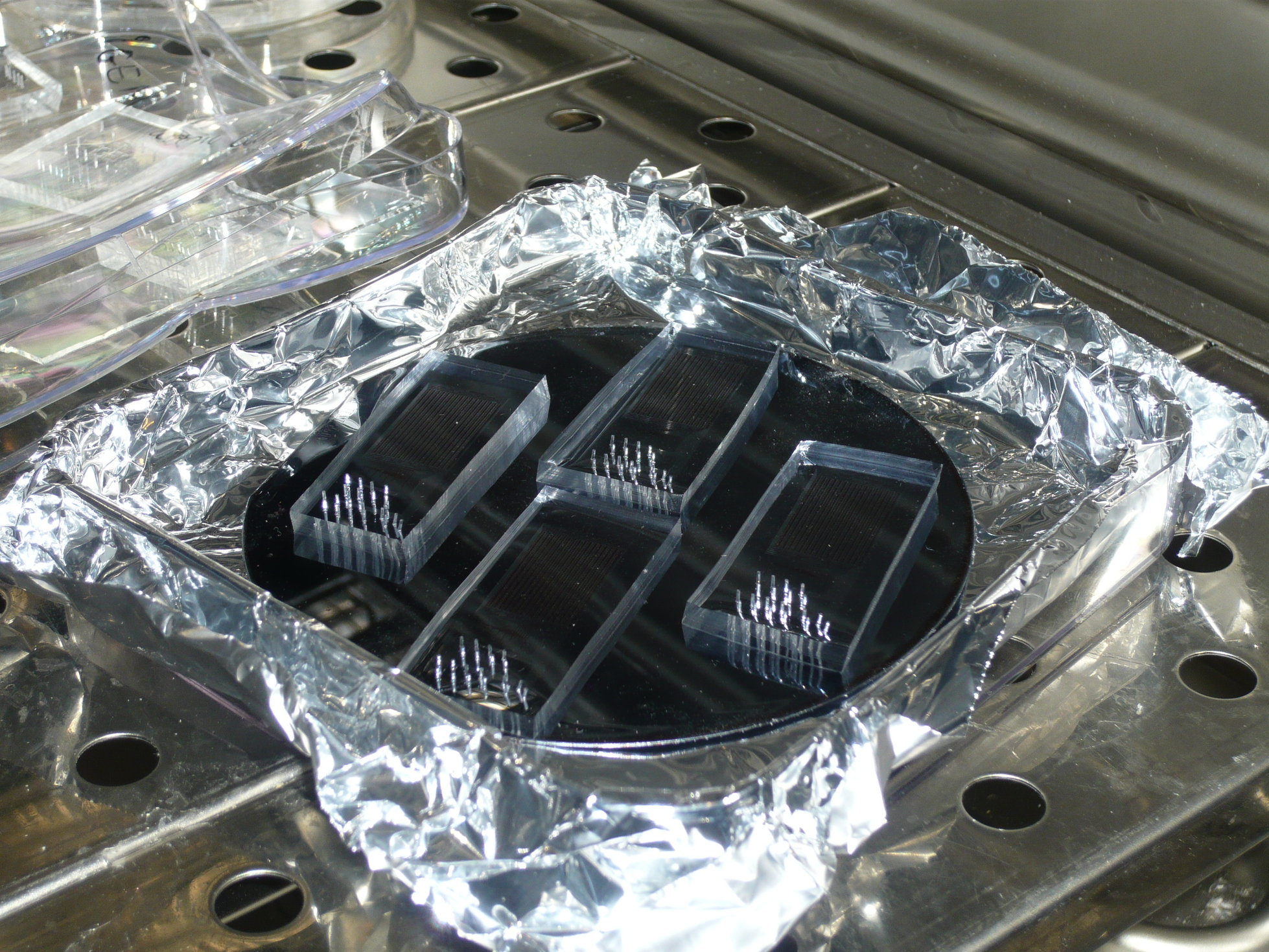
If your lab is equipped, you should have no problem replicating our protocol for MITOMI chip fabrication, illustrated here by Lilia:
1) Place molds into a TMCS vapor chamber for at least 20min
2a) Control layer mixture
2b) Mix for 1 minute, degas for 2 minutes (standard protocol)
2c) Pour onto control layer mold and place mold in vacuum chamber for at least 20min
3a) Flow layer mixture
3b) Mix for 1 minute and degas for 2 minutes (standard protocol)
3c) Spin coat onto flow layer
4) Remove control layer mold from vacuum chamber, making sure no bubbles are left on the surface (remove with a toothpick if you see some )
5) Place the control and flow layer in a 80C convection oven and incubate for 30 minutes (timing is critical here!)
6a) Remover wafers both layers from the oven, cut out control layer
6b) Punch holes
6c) Align control to the flow layer
7) Put aligned device back into 80C oven and incubate for at least 90 minutes (and here you can increase the baking time)
8a) Remove devices from oven
8b) Cut them out
8c) Punch flow layer holes and cut the edges through the flow layer
Before use the chip should be aligned to the epoxy-treated glass slide. There can be DNA, bacteria or other substances spotted on it (in case of MITOMI device we spot different variants of the tetO sequence in this project).
 "
"
