Team:Cornell/Description
From 2011.igem.org
(→Microfluidic Device) |
Rockyshell92 (Talk | contribs) (→Microfluidic Device) |
||
| Line 16: | Line 16: | ||
=Microfluidic Device= | =Microfluidic Device= | ||
| - | + | [[file:Microfulidics_section2_Cornell2011_(3).jpg|965px|left]] | |
<html><img src="http://i1214.photobucket.com/albums/cc481/mg573/comsol%20models/MuchNicerChipRenderFinal_Color_Output.png"></img> | <html><img src="http://i1214.photobucket.com/albums/cc481/mg573/comsol%20models/MuchNicerChipRenderFinal_Color_Output.png"></img> | ||
Revision as of 23:54, 28 October 2011
Project Description |
Future Directions |
Business Development |
Outreach/HP |
Safety
Contents |
The BioFactory
Cornell’s BioFactory aims to develop a simple and efficient method for the construction of enzyme-immobilized surfaces capable of multi-step chemical reactions.
As more chemical production techniques begin to utilize enzymatic reactions, genetic engineers must consider ways to resolve competing side reactions and the toxic accumulation of intermediates, reduce purification costs, and correctly express non-native enzymes or proteins in bacteria. In some cases, such challenges could be more easily resolved by simply extracting the molecular metabolic mechanisms and produce the target compound in a cell-free environment. We believe a cell-free system for biosynthesis can resolve these issues and still use the power of bacteria to help build devices capable of producing complex organic compounds.
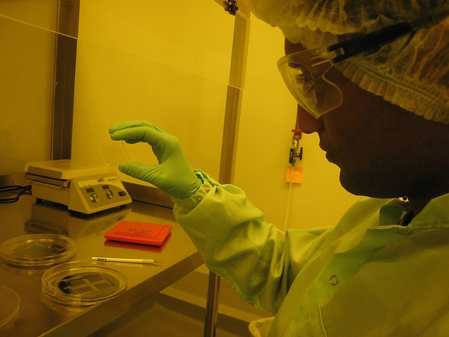
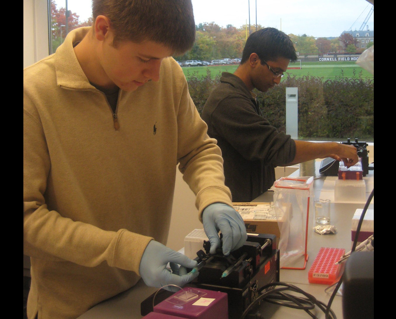
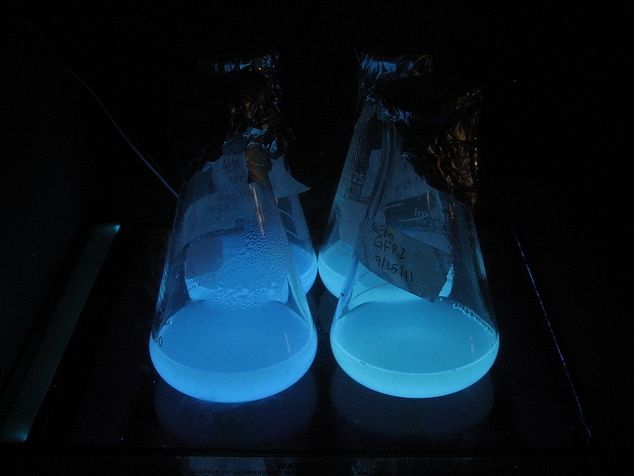
Over the summer, Cornell's iGEM team engineered strains of E. Coli to produce modified enzymes from the biosynthetic pathway of Violacein which were immobilized on the surface of microfluidic devices and capable of converting an initial feed of substrate into prodeoxyviolacein, a direct intermediate of the violacein pathway. The microfluidic chips were designed, built and tested in the lab using Cornell’s modern cleanroom and nanofabrication facilities. We additionally designed and began construction of a light-induced apoptosis system capable of lysing bacteria cultures, producing the necessary enzymes without the use of expensive reagents or extensive protocols.
Microfluidic Device
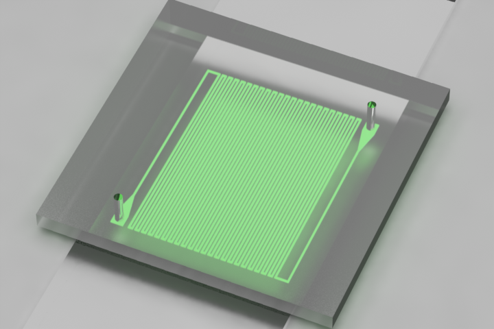
Overview:
In order to develop a scalable synthetic pathway the team required a means to apply enzymes
to proteins extracted from lysis.
This means would have to:
- Provide large enzyme exposure area within a small volume.
- Allow for scalability for industrial application.
- Be able to accommodate a system of separate enzymes as components of a chosen biosynthetic pathway.
- Be relatively simple and inexpensive
After a series of brainstorming and development sessions during the spring of 2011, the team
decided to move forward with the creation of a microfluidic device.
Final Chip Design (7/3/2011 - 7/6/2011)
Summary:
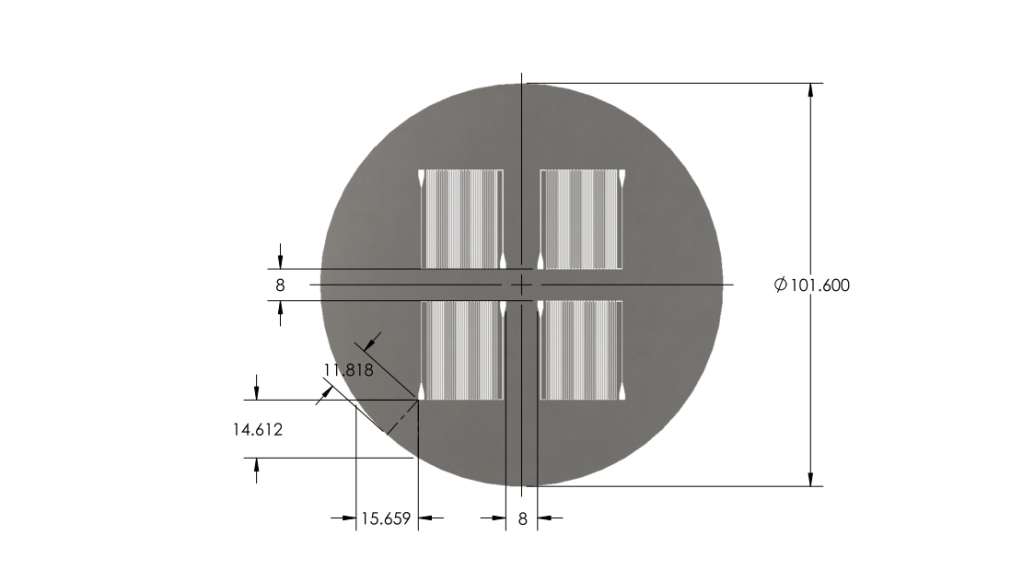
Optimized chip size to fit 4 chips on a 4'' diameter wafer.
After discussion, changed channel dimensions back to narrow safe limits of printing machine: 200 microns wide, 200 micron spacing.
Channel margins changed to limit of safe margin for wafer size.(1cm from edge)
Inlet/outlet positioning was changed to prevent channel damage when punching inlet/outlet holes.
Final Design was approved for printing.
Solidworks Sketch converted to DXF in Solidworks. Edited in Modo. Converted to GDS using LinkCAD and printed to mask.
Basis for Revision:
- Channels dimensions needed to balance space-savings and safe-print.
- Team wanted to print as many chips in as little space as possible.
- Team aimed to minimize damage when punching inlet/outlet holes.
Features:
Material:
We chose to create our microfluidic chip out of Polydimethylsiloxane
(PDMS) because of its extensive use in biologically related
microfluidic research. PDMS is an optically clear, nontoxic,
nonflammable and inert material that is ideal for working with
biological material. It is also a cost efficient material that can
easily be fabricated into a microfluidic device.
Inlet/Outlet
- Changed inlet/outlet position to reduce wasted space and reduce loss of chips
Channel
Dimensions
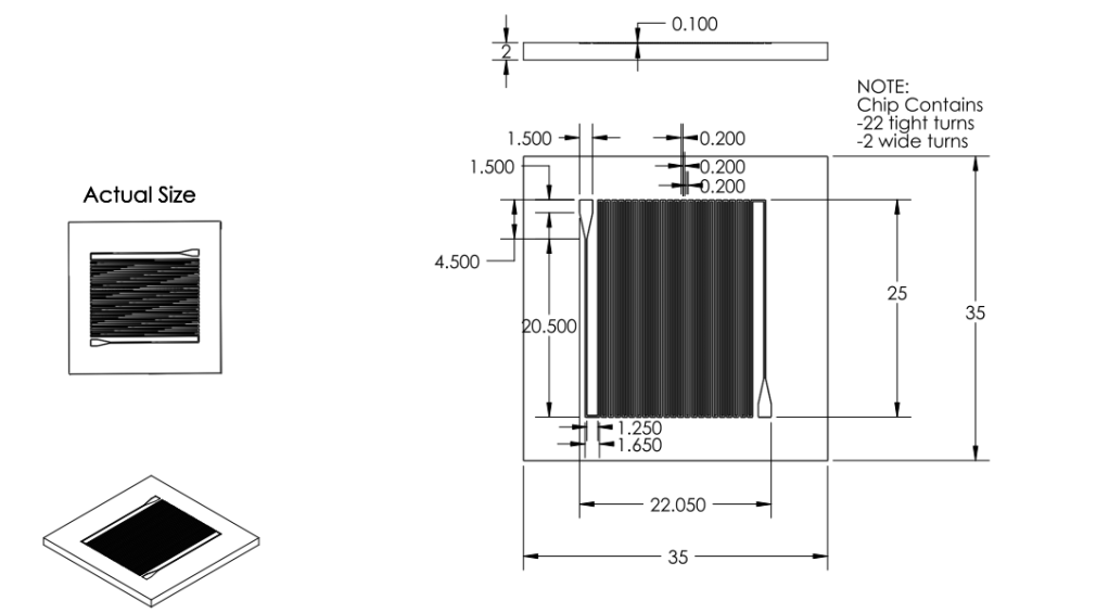
- Channel width changed to 200 microns.
- Channel spacing changed to 200 microns.
- Channel depth changed to 100 microns.
Overall Dimensions
- Reduced chip print dimensions to 22.05mm by 25.00mm. Fits 4 safely on a 4'' diameter wafer. (101.6 mm diameter)
Mask
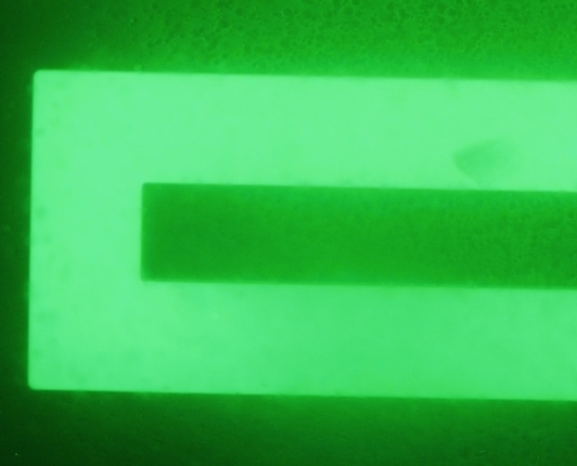
- Developed. Specifications drawing in Images below.
DXF to GDS File:
 "
"


