Team:EPF-Lausanne/Protocols/Master microfabrication for PDMS replica molding
From 2011.igem.org
(Difference between revisions)
| (4 intermediate revisions not shown) | |||
| Line 1: | Line 1: | ||
| - | {{:Team:EPF-Lausanne/Templates/ProtocolHeader|title=Master fabrication for PDMS replica | + | {{:Team:EPF-Lausanne/Templates/ProtocolHeader|title=Master fabrication for PDMS replica moulding}} |
| + | The protocol below is for a two lithographic steps process, for the case when two different channel heights are needed. | ||
| + | If one height is needed, as in the case of MITOMI chips fabrication, only one resist configured during one lithographic process is necessary. | ||
| + | Process Flow: | ||
| + | The images represent the wafer cross section during the main technological steps: | ||
| + | |||
| + | [[File:Microchannel fabrication steps - 1.png]] | ||
| + | [[File:Microchannel fabrication steps - 2.png]] | ||
| + | |||
| + | |||
| + | <html> | ||
| + | <embed type="application/x-shockwave-flash" src="https://picasaweb.google.com/s/c/bin/slideshow.swf" width="600" height="400" flashvars="host=picasaweb.google.com&captions=1&noautoplay=1&hl=en_US&feat=flashalbum&RGB=0x000000&feed=https%3A%2F%2Fpicasaweb.google.com%2Fdata%2Ffeed%2Fapi%2Fuser%2F114670117111403230486%2Falbumid%2F5654374714730282977%3Falt%3Drss%26kind%3Dphoto%26hl%3Den_US" pluginspage="http://www.macromedia.com/go/getflashplayer"></embed> | ||
| + | </html> | ||
{{:Team:EPF-Lausanne/Templates/Footer}} | {{:Team:EPF-Lausanne/Templates/Footer}} | ||
Latest revision as of 00:45, 22 September 2011
Master fabrication for PDMS replica moulding
Back to protocols.The protocol below is for a two lithographic steps process, for the case when two different channel heights are needed. If one height is needed, as in the case of MITOMI chips fabrication, only one resist configured during one lithographic process is necessary.
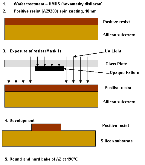
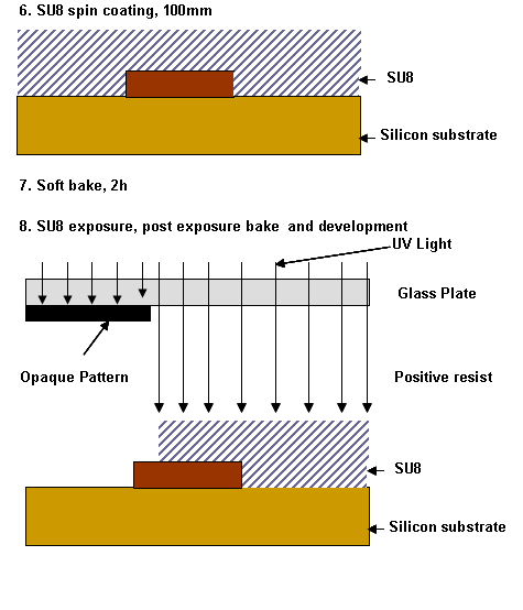
Process Flow:
The images represent the wafer cross section during the main technological steps:
 "
"

