Team:EPF-Lausanne/Tools/Microfluidics/HowTo1
From 2011.igem.org
(→PDMS chip fabrication) |
|||
| (21 intermediate revisions not shown) | |||
| Line 1: | Line 1: | ||
| - | {{:Team:EPF-Lausanne/Templates/MicrofluidicsHeader|title=Microfluidics | + | {{:Team:EPF-Lausanne/Templates/MicrofluidicsHeader|title=Microfluidics How-To Part I: Making Chips}} |
There are three main steps in the making of a microfluidic chip: | There are three main steps in the making of a microfluidic chip: | ||
| Line 8: | Line 8: | ||
Designing chips is a subtle task, but for many applications one can re-use an existing design. Moulds are also usually made using expensive equipment found in clean rooms. | Designing chips is a subtle task, but for many applications one can re-use an existing design. Moulds are also usually made using expensive equipment found in clean rooms. | ||
| - | If you have a clean room, somebody there will be able to train you on fabrication, based on our [ | + | If you have a clean room, somebody there will be able to train you on fabrication, based on our [https://2011.igem.org/Team:EPF-Lausanne/Protocols/Master_microfabrication_for_PDMS_replica_molding protocols]. If you do not, you can try to experiment with making moulds out of laser machined metal, but it will probably be easier to order them. Stanford offers a [http://www.stanford.edu/group/foundry/index.html foundry service]. |
Moulding is the most common task: it must be done over and over again, as the chips are usually single use. Again, this requires specific equipment not usually found in a bio lab. So unless a friendly lab in your neighbourhood is equipped, you'll probably have to order the chips. | Moulding is the most common task: it must be done over and over again, as the chips are usually single use. Again, this requires specific equipment not usually found in a bio lab. So unless a friendly lab in your neighbourhood is equipped, you'll probably have to order the chips. | ||
| + | |||
| + | ==Making a Mould== | ||
| + | |||
| + | Our moulds are made by photolithography: a layer of AZ or SU-8 resist is spin-coated onto a silicon wafer, then exposed, developed, | ||
| + | and etched, to only a positive image of the channels in resist. The mould is thus a plane of silicon, with features made in photoresist. To provide the mould walls, we place the wafer in an aluminium-foil-lined petri dish. | ||
| + | |||
| + | The complete protocol for the clean room fabrication of the mold can be found [[Team:EPF-Lausanne/Protocols/Master_microfabrication_for_PDMS_replica_molding|here]]. Many pictures of the fabrication process in our clean rooms are in our [https://picasaweb.google.com/114670117111403230486/CleanRoomMouldFabrication?authuser=0&feat=directlink picasa gallery] | ||
| + | |||
| + | [[File:EPFL-AZ-Robot.JPG|thumb|left|AZ photolithography robot.]] | ||
| + | [[File:EPFL-Mask-Aligner.JPG|thumb|left|Changing masks on the mask aligner.]] | ||
| + | [[File:EPFL-Wetbench.JPG|thumb|left|Wet bench for SU8 development.]] | ||
==PDMS== | ==PDMS== | ||
| - | PDMS or poly(dimethylsiloxane), informally known as ''silicone'', is a cross-linkable elastomer. In | + | PDMS or poly(dimethylsiloxane), informally known as ''silicone'', is a cross-linkable elastomer. In layman's terms, it is a transparent rubber-like material. |
[[File:EPFL-PDMS-chips.JPG|thumb|right|250px|PDMS chips: the four rectangular transparent blocs]] | [[File:EPFL-PDMS-chips.JPG|thumb|right|250px|PDMS chips: the four rectangular transparent blocs]] | ||
| Line 30: | Line 41: | ||
For more information on PDMS chip fabrication: Mcdonald, J.C. et al. Fabrication of microfluidic systems in poly (dimethylsiloxane). Electrophoresis 21, 27–40(2000). | For more information on PDMS chip fabrication: Mcdonald, J.C. et al. Fabrication of microfluidic systems in poly (dimethylsiloxane). Electrophoresis 21, 27–40(2000). | ||
| - | ==Making | + | == Making the Chips == |
| - | + | ||
| - | + | ||
| - | + | ||
| - | + | ||
| - | + | ||
| - | + | ||
| - | + | ||
| - | + | ||
| - | + | ||
| - | + | ||
| - | + | ||
| - | + | ||
| - | + | ||
MITOMI chips are two layer devices. A thick upper layer is imprinted with the flow channels (those that will contain reagents) and a thin bottom layer is imprinted with the control channels (used to actuate on-chip valves). The role of each layer is explained further in [[Team:EPF-Lausanne/Tools/Microfluidics/HowTo2|Part II]]. | MITOMI chips are two layer devices. A thick upper layer is imprinted with the flow channels (those that will contain reagents) and a thin bottom layer is imprinted with the control channels (used to actuate on-chip valves). The role of each layer is explained further in [[Team:EPF-Lausanne/Tools/Microfluidics/HowTo2|Part II]]. | ||
| - | Casting PDMS involves mixing a precursor and a curing agent (sold as | + | Casting PDMS involves mixing a precursor and a curing agent (sold as the Sylgard 184 kit by Dow Corning), degassing, pouring into the mould (or spin-coating onto the wafer for the thin layers), and partial curing at 80°C. After curing, holes are punched through the flow layer, to allow plugging in of external tubing (again, see part II). The two layers are then superposed and aligned by hand, so that the valves from the control layer overlap the correct channels on the flow layer. |
After alignment, curing is finalised. This fully solidifies the chip and ensures a strong bond between the two layers. After curing, holes are punched through to the flow layer. For most chips, the last step is to bond them them to a glass microscope slide, following a plasma surface treatment if strong bonding is required. In the case of the MITOMI chips, they are instead aligned onto a spotted array from a DNA library. At this point, the chip is ready to use. | After alignment, curing is finalised. This fully solidifies the chip and ensures a strong bond between the two layers. After curing, holes are punched through to the flow layer. For most chips, the last step is to bond them them to a glass microscope slide, following a plasma surface treatment if strong bonding is required. In the case of the MITOMI chips, they are instead aligned onto a spotted array from a DNA library. At this point, the chip is ready to use. | ||
| Line 53: | Line 51: | ||
The specifics of each step are explained in our [[Team:EPF-Lausanne/Protocols/PDMS_two_layer_device_fabrication|protocol]] for MITOMI chip fabrication. The process is illustrated on our [https://picasaweb.google.com/114670117111403230486/ChipFab_steps?authuser=0&feat=directlink Picasa gallery]. More pictures of chip fabrication are also available [https://picasaweb.google.com/114670117111403230486/ChipFabMITOMI?authuser=0&feat=directlink here]. | The specifics of each step are explained in our [[Team:EPF-Lausanne/Protocols/PDMS_two_layer_device_fabrication|protocol]] for MITOMI chip fabrication. The process is illustrated on our [https://picasaweb.google.com/114670117111403230486/ChipFab_steps?authuser=0&feat=directlink Picasa gallery]. More pictures of chip fabrication are also available [https://picasaweb.google.com/114670117111403230486/ChipFabMITOMI?authuser=0&feat=directlink here]. | ||
| - | + | [[File:EPFL-Pouring.JPG|thumb|left|Pouring PDMS. Note the vacuum chamber for degassing.]] | |
| - | + | [[File:EPFL-Cutout.JPG|thumb|left|Cutting out the chip after curing.]] | |
| - | + | [[File:EPFL-Align.JPG|thumb|left|The two layers have to be aligned by hand.]] | |
{{:Team:EPF-Lausanne/Templates/Footer}} | {{:Team:EPF-Lausanne/Templates/Footer}} | ||
Latest revision as of 03:27, 22 September 2011
Microfluidics How-To Part I: Making Chips
Microfluidics Main | How-To Part I | How-To Part II | TamagotchipThere are three main steps in the making of a microfluidic chip:
- Designing the chip
- Making a mould
- Moulding PDMS chips.
Designing chips is a subtle task, but for many applications one can re-use an existing design. Moulds are also usually made using expensive equipment found in clean rooms. If you have a clean room, somebody there will be able to train you on fabrication, based on our protocols. If you do not, you can try to experiment with making moulds out of laser machined metal, but it will probably be easier to order them. Stanford offers a [http://www.stanford.edu/group/foundry/index.html foundry service].
Moulding is the most common task: it must be done over and over again, as the chips are usually single use. Again, this requires specific equipment not usually found in a bio lab. So unless a friendly lab in your neighbourhood is equipped, you'll probably have to order the chips.
Making a Mould
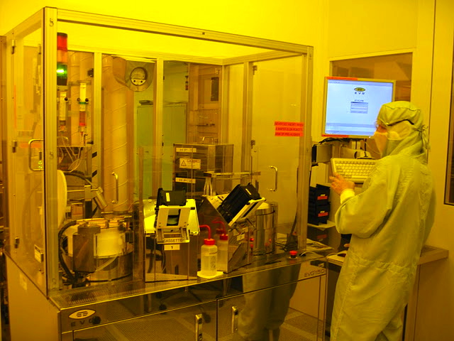
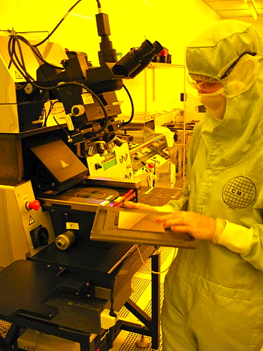
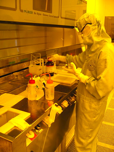
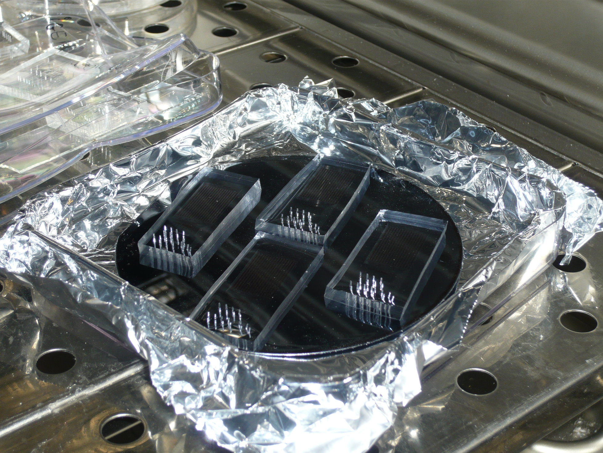
Our moulds are made by photolithography: a layer of AZ or SU-8 resist is spin-coated onto a silicon wafer, then exposed, developed, and etched, to only a positive image of the channels in resist. The mould is thus a plane of silicon, with features made in photoresist. To provide the mould walls, we place the wafer in an aluminium-foil-lined petri dish.
The complete protocol for the clean room fabrication of the mold can be found here. Many pictures of the fabrication process in our clean rooms are in our picasa gallery
PDMS
PDMS or poly(dimethylsiloxane), informally known as silicone, is a cross-linkable elastomer. In layman's terms, it is a transparent rubber-like material.
It is used for the fabrication of microfluidic chips for many reasons:
- Being flexible, it is easy to cast, and conforms to imperfect surfaces.
- It accurately reproduces micro-scale patterns.
- It is transparent down to UV light, allowing easy optical microscope observation and enabling fluorescence techniques of UV-range absorption.
- It is non-toxic, allowing on-chip cell culture.
- It can seal reversibly or irreversibly to itself or glass, allowing the fabrication of multi-layer devices, and strong bonding to glass slides.
- Its surface chemistry can be controlled.
- It is oxygen permeable, allowing air to diffuse out of the channels through the chip when the channels are filled.
For more information on PDMS chip fabrication: Mcdonald, J.C. et al. Fabrication of microfluidic systems in poly (dimethylsiloxane). Electrophoresis 21, 27–40(2000).
Making the Chips
MITOMI chips are two layer devices. A thick upper layer is imprinted with the flow channels (those that will contain reagents) and a thin bottom layer is imprinted with the control channels (used to actuate on-chip valves). The role of each layer is explained further in Part II.
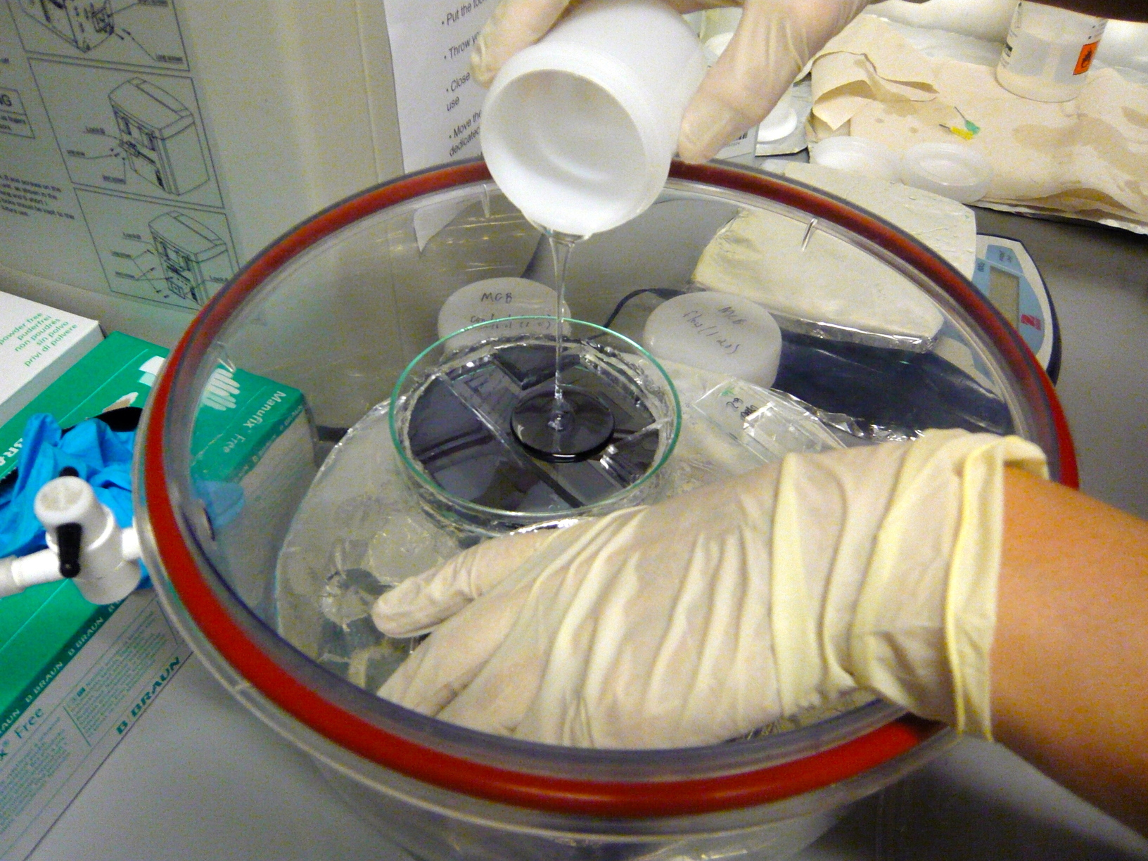
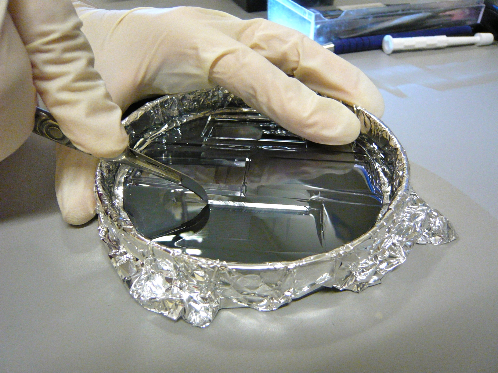
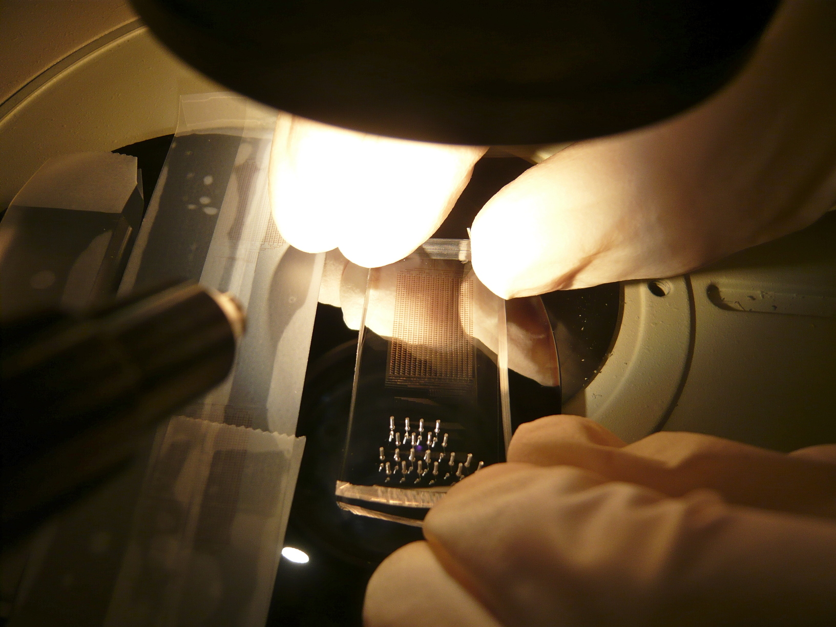
Casting PDMS involves mixing a precursor and a curing agent (sold as the Sylgard 184 kit by Dow Corning), degassing, pouring into the mould (or spin-coating onto the wafer for the thin layers), and partial curing at 80°C. After curing, holes are punched through the flow layer, to allow plugging in of external tubing (again, see part II). The two layers are then superposed and aligned by hand, so that the valves from the control layer overlap the correct channels on the flow layer.
After alignment, curing is finalised. This fully solidifies the chip and ensures a strong bond between the two layers. After curing, holes are punched through to the flow layer. For most chips, the last step is to bond them them to a glass microscope slide, following a plasma surface treatment if strong bonding is required. In the case of the MITOMI chips, they are instead aligned onto a spotted array from a DNA library. At this point, the chip is ready to use.
The specifics of each step are explained in our protocol for MITOMI chip fabrication. The process is illustrated on our Picasa gallery. More pictures of chip fabrication are also available here.
 "
"
